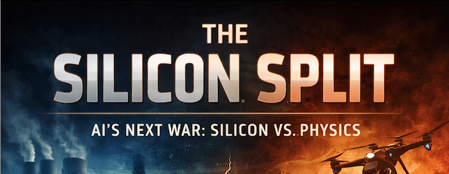
The next war over AI will not be fought in model weights. It will be fought in silicon. And the winner will be determined not by who has the best algorithm, but by who owns the physics.
Software-based AI running on general-purpose processors is a temporary historical accident. It works the way the early internet worked over phone lines: functional, transformative, and fundamentally mismatched to the medium. We are now entering the era where AI migrates from borrowed hardware into purpose-built substrate, and almost nobody is talking about what this means for the power structure that was just starting to form around the current paradigm.
Here is why this migration is inevitable. A general-purpose CPU spends the majority of its energy on things that have nothing to do with intelligence. Instruction fetching. Branch prediction. Speculative execution. Cache coherency protocols. A modern processor is an elaborate bureaucracy where the actual math of a neural network is a small tenant in a large building full of overhead. A custom chip designed to do nothing but matrix multiplications and attention computations strips all of that away. The same operation that costs one unit of energy on a GPU costs a tenth or a hundredth on a purpose-built ASIC. At the scale of a datacenter running trillions of inference operations per day, this is not an optimization. It is the difference between economic viability and bankruptcy.
But energy is not even the deepest reason. Memory bandwidth is.
The transformer architecture has a brutal secret that no amount of software cleverness can fix. Attention requires moving enormous volumes of data between where it is stored and where it is computed. On conventional hardware, memory lives in one place and compute lives in another, connected by a bus that becomes the bottleneck for everything. This is the Von Neumann wall, and it has been the binding constraint on computing for seventy years. Software cannot route around physics. You cannot optimize your way past the speed of electrons moving through copper traces on a motherboard. The only solution is to put the computation where the memory already is. Processing-in-memory. Near-memory compute. Architectures where the data never moves because the math happens at the point of storage. This requires new silicon. No driver update will deliver it.
Then there is numerical precision. Your GPU faithfully implements IEEE floating point because it was designed for a world where rendering a pixel incorrectly was unacceptable. AI does not need that contract. A transformer will produce nearly identical outputs whether you compute in 32-bit floating point, 16-bit, 8-bit, or in some cases 4-bit. Custom AI hardware can implement exotic number formats natively, formats that do not exist in any software library because no general-purpose chip has ever supported them. FP8. FP4. Block floating point. Logarithmic number systems. Each of these buys you a 2x to 8x improvement in throughput for free, because you are doing less work per operation and the model does not care. Software emulation of these formats eats the gains. Only native silicon makes them real.
Now extend this logic to the extremes and see where it leads.
At the edge, the implications are liberating. A purpose-built inference chip consuming two watts can run a meaningful model on a device with no fan, no cloud connection, and no terms of service. Your phone. Your car. Your glasses. A medical device implanted in your body. The same model that requires a rack-mounted GPU server today could run on a chip the size of a fingernail tomorrow, not because the model shrank, but because the silicon was sculpted to fit it exactly. This is how Tier 2 intelligence, the human-level local AI from the previous discussion, breaks free of the laptop form factor and becomes ubiquitous. Dedicated hardware is what makes private, persistent, always-on intelligence physically possible in objects you carry.
At the top, the implications are concentrating. And this is the part that requires honest accounting, because the hardware case for superintelligence is not just an amplified version of the edge story. It is a different kind of engineering entirely, governed by constraints that do not yield to the same tricks.
Start with the raw arithmetic. A dense trillion-parameter model, even on purpose-built silicon, requires holding those parameters somewhere and streaming them through compute units on every forward pass. Custom number formats help. FP4 and aggressive quantization can compress a trillion parameters into 500GB or less. But a single chip, no matter how specialized, holds at most tens of gigabytes of on-die memory. A wafer-scale chip like Cerebras pushes this further, tiling an entire silicon wafer with cores and on-chip SRAM, eliminating the need to go off-chip for a large fraction of the weights. But even a full wafer tops out. A trillion-parameter superintelligence at any useful precision does not fit on one wafer. It is distributed across dozens or hundreds of chips by necessity, which means the binding constraint shifts from memory bandwidth within a chip to interconnect bandwidth between chips. The speed of light across a fiber optic cable between racks becomes a hard ceiling on how fast the system can think. This is not a software problem. It is not even a chip design problem. It is a facility design problem. The physical layout of a building, the length of copper and glass between nodes, the topology of the network fabric, all become architectural decisions about intelligence itself.
Then there is power. A single purpose-built AI accelerator might draw 300 to 700 watts. A superintelligence system running thousands of these accelerators in parallel, executing long-horizon reasoning chains across a model that spans hundreds of chips, draws megawatts. Not kilowatts. Megawatts. The facilities being built today to house these systems require dedicated substations, direct connections to power plants, and in some cases entirely new energy infrastructure at the site. Liquid cooling is not optional. It is the baseline. Some next-generation designs are exploring immersion cooling, submerging entire server racks in dielectric fluid, because air cannot remove heat fast enough from silicon running at these densities. Others are investigating co-location with nuclear microreactors, not as a green energy talking point but as a physical engineering requirement because the grid cannot deliver enough power to a single building.
Custom silicon makes all of this more efficient, but it does not make it small. It does the opposite. It makes the investment case for building cathedral-scale AI facilities overwhelming, because purpose-built hardware extracts so much more intelligence per watt that the returns to concentration become enormous. A hyperscaler running superintelligence on custom ASICs is not just faster than one running on general-purpose GPUs. It is operating at a fundamentally different cost curve. The efficiency gains from dedicated hardware do not democratize the top tier. They subsidize it for the entities large enough to build the facilities in the first place.
And the most radical hardware approaches push this concentration further. Photonic computing performs matrix multiplication at the speed of light using interference patterns in silicon waveguides. Analog compute arrays encode weights as electrical charges on memristive crossbars, performing an entire matrix-vector multiply in a single clock cycle with near-zero energy. Superconducting circuits operating near absolute zero switch at hundreds of gigahertz with negligible power dissipation. Each of these offers 100x to 1000x efficiency gains over digital logic for specific AI workloads. None of them are consumer technologies. A photonic AI chip requires precision fabrication of optical components at nanometer tolerances. A cryogenic superconducting array requires a liquid helium cooling plant. These are physics experiments masquerading as products, and they will be deployed exclusively in facilities that cost billions to build, operated by organizations that can amortize that cost across millions of paying users.
The result is that purpose-built hardware simultaneously enables two opposite things. It liberates local intelligence by making edge inference radically cheaper. And it entrenches centralized superintelligence by making the cost curve of the largest systems steeper, not flatter, rewarding scale and concentration at every level. The gap between Tier 2 and Tier 3 will not be measured in model parameters or benchmark scores. It will be measured in the physics each tier can access. Your local chip does digital math on a few billion parameters. The cathedral does analog and photonic computation across trillions. It is not a difference of degree. It is a difference of substrate.
This creates a new axis of power that did not exist in the software-only world.
When AI was purely a software problem, the barrier was data and training compute, both of which are expensive but ultimately fungible. Money could buy GPUs anywhere. The knowledge of how to train a model was diffusing rapidly. Open weights meant that capability, once created, could not be uncreated. But when AI becomes a hardware problem, the barriers become physical. Semiconductor fabrication. Exotic materials. Photonic integration. Cryogenic infrastructure. These do not diffuse like code on GitHub. They concentrate in whoever controls the most advanced fabs, the most specialized manufacturing, and the longest-horizon capital investment. The companies and nations that own the next generation of AI-specific silicon will own a capability advantage that cannot be copied by downloading a file.
This is already happening. It is happening in the TPU program at Google, which has been quietly building custom AI silicon for nearly a decade, creating an inference cost advantage that no amount of open-source software can neutralize. It is happening in the semiconductor export controls that treat advanced chips as strategic weapons. It is happening in every startup designing neuromorphic processors, photonic accelerators, and analog compute arrays behind closed doors with defense funding and no intention of selling to consumers.
The question is not whether AI moves into dedicated hardware. That is settled by thermodynamics. The question is the same one from the previous discussion, sharpened to a finer point: which tier of intelligence gets which tier of silicon? If purpose-built edge chips keep advancing, Tier 2 intelligence, your private, sovereign, continuously-learning cognitive partner, becomes smaller, cheaper, and more capable every year, embedded in everything, loyal to no one but the person who owns it. If the most transformative hardware breakthroughs remain locked in hyperscaler facilities, Tier 3 superintelligence becomes not just expensive to access but physically impossible to replicate.
The split between those who own their intelligence and those who rent it was always going to be defined by hardware. Software was the opening act. Silicon is the main event.
The people designing these chips right now are making decisions that will determine the topology of cognitive power for the next fifty years. Almost none of those decisions are being made in public. Almost all of them are being made by people whose economic incentive is to keep the most powerful silicon behind walls, metered and monitored, rented by the hour, revocable at will.
The physics is not the problem. The physics is generous. It offers a path to sovereign intelligence on a chip you hold in your hand. The problem is the same one it has always been: who builds the chip, and who gets to buy it.